- Operating principle and configuration of a linear regulator
1. Linear regulator operating principle
The following offers a description of the operating principle of a linear regulator. The figure below shows a model providing a simplified view of a linear regulator.
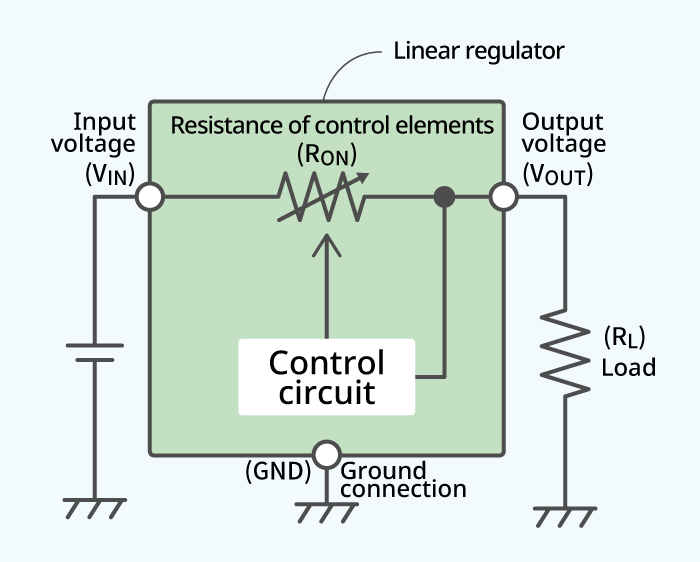
A linear regulator can maintain a steady output voltage (VOUT) by adjusting the resistance of control elements (RON) to compensate for input voltage (VIN) and load (RL) changes. Details of internal configuration and control are explained in “2. Internal configuration of a linear regulator.”
What is heat loss?
We will use this model to consider the “heat loss” that always occurs during operation of a linear regulator. The following is assumed:
Input voltage (VIN)=3.0V, output voltage (VOUT)=1.0V, output current (IOUT)= 100mA.
In this case, power on the input side of the linear regulator is about 0.3W and as 0.1W is output, the difference between the input and output side is about 0.2W.
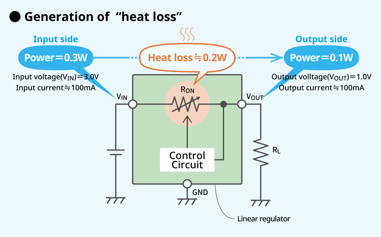
“Heat loss” in the linear regulator is what accounts for this difference, most of which is self-heating through control elements, and the remainder is consumed by the self-current consumption of the linear regulator. The larger the difference between input and output voltage and the greater the load current, the larger the heat loss will be.
For this reason, thermal design is required in the use of a linear regulator.
IC power dissipation is an important factor in implementing thermal design. IC power dissipation indicates the allowable heat loss value.
If the IC is used in operating conditions that exceed its power dissipation, the guaranteed operation temperature of the IC will be exceeded.
ABLIC provides a “Thermal simulation service” to support thermal design using ABLIC power supply ICs under customer usage conditions. This Thermal simulation service helps lower risk of thermal design at the customer development stage.
Please contact our sales representatives for using our Thermal simulation service.
2. Internal configuration of a linear regulator
Let's take a closer look at the internal configuration of a linear regulator.
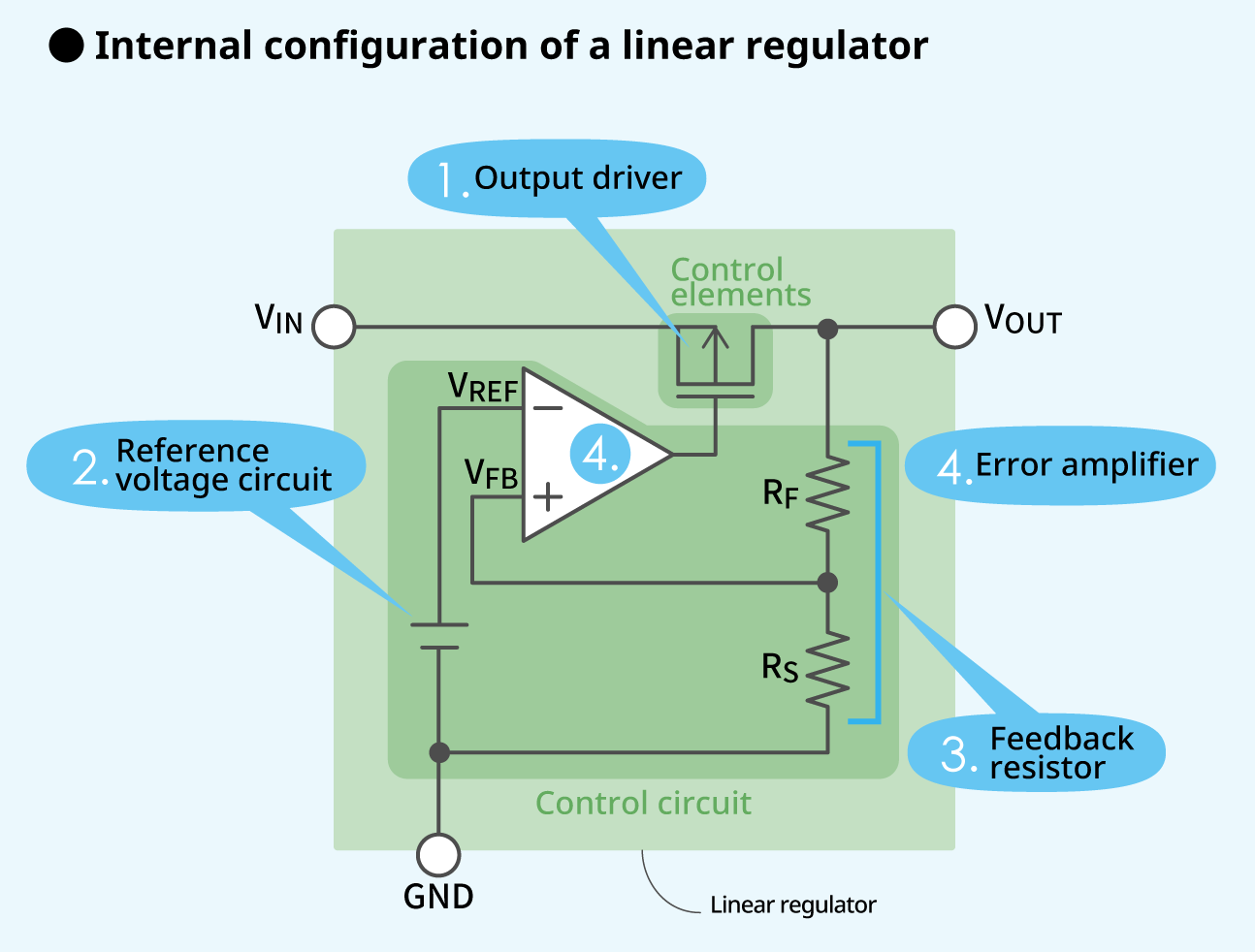
1. Output driver
Current passing from the input voltage (VIN) side to the output voltage (VOUT) side passes through the output driver.
For this reason, the major part of linear regulator heat loss occurs in the output driver.
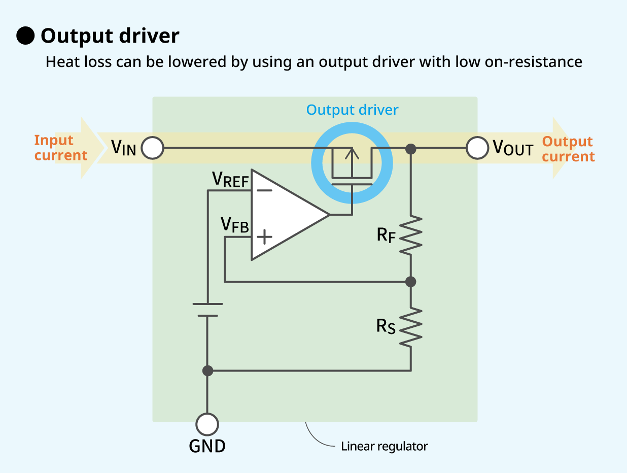
Using an excellent output driver, that is, an output driver with low on-resistance, it will be possible even for a regulator with high output current to deliver the required output voltage from a low input voltage while also lowering heat loss.
A linear regulator that can deliver the required output voltage even at a low difference between input and output voltage is called an LDO regulator.
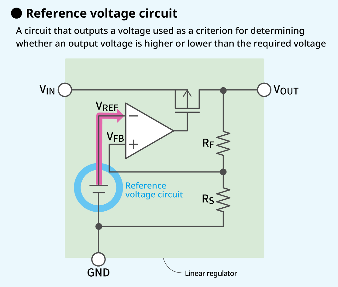
2.Reference voltage circuit
A reference voltage circuit outputs a voltage (= reference voltage, VREF) used as a standard to the error amplifier to determine whether an output voltage (VOUT) is higher or lower than the required voltage.
Since it is used as a criterion for testing output voltages, it is essential it is a steady, precise voltage. It must output a steady voltage without being impacted by input voltage, temperature and other surrounding environmental factors.
3. Feedback resistor
A feedback resistor is connected between the output pin and ground (GND) to divide the output voltage (VOUT) by the RF and RS resistors to output the resulting voltage (VFB) to an error amplifier.
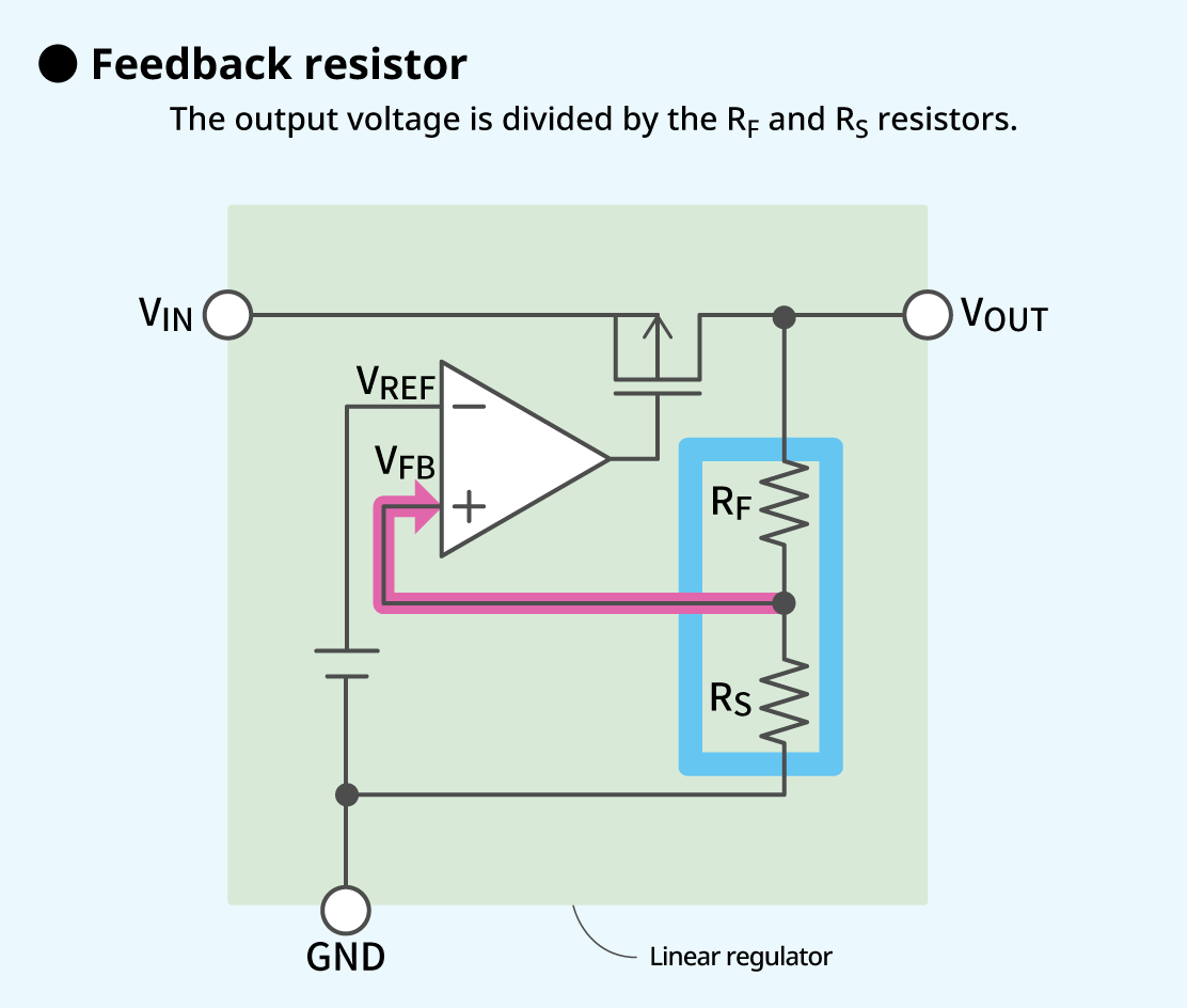
The feedback resistor is required to output the voltage resulting (VFB) from dividing the output voltage (VOUT) by the required voltage to an error amplifier. Even if the criterion (VREF) is stable, the error amplifier will not be able to make a correct assessment unless it is able to correctly recognize the state of the output voltage (VFB).
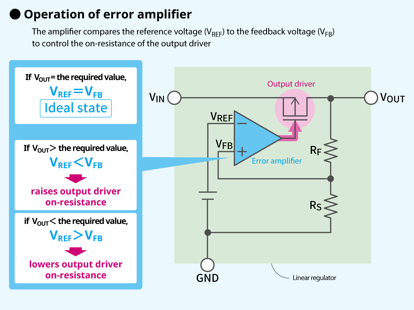
4. Error amplifier
The error amplifier compares the reference voltage (VREF) output by the reference voltage circuit and the feedback voltage (VFB) divided by the feedback resistor to control the output driver on-resistance to ensure the output voltage (VOUT) is maintained at the required voltage.
The error amplifier controls the output driver in the following manner. When VOUT is higher than the required value (VREF < VFB), the error amplifier raises the on-resistance of the output driver and when VOUT is lower than the required value (VREF > VFB), it lowers output driver on-resistance.
For details on error amplifiers, refer to “What is an operational amplifier?”