What is a Voltage Reference?

Table of Contents
ABLIC's Automotive Voltage References
1. What is a Voltage Reference?
Role and Types of Voltage References
Electronic devices and sensor equipment operate by sensing analog quantities such as voltage, current, temperature, and position, and converting these analog values into corresponding voltage signals.
To perform control using voltage, a stable reference voltage is required, separate from the measured signal voltage. This reference voltage is used, for example, as a standard for accurately comparing analog sensor output voltages or for analog-to-digital signal conversion.
The standard voltage is generated by the voltage reference, which is indispensable for maintaining measurement accuracy.
A voltage reference is a linear regulator capable of maintaining a highly stable output voltage. Compared with an LDO, which is also a linear regulator, the main differences are as follows.
| Type | Main Application | Output Voltage Accuracy | Features |
|---|---|---|---|
| Voltage Reference | Reference voltage for applications | High | Maintains high-precision even when the power supply voltage or ambient temperature fluctuates. |
| LDO | Power supply voltage for applications | General | Capable of supplying large current with high efficiency. |
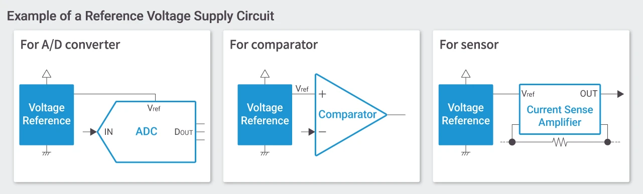
Voltage references are widely used as the reference voltage sources for components requiring high-precision, such as A/D converters (ADC), comparators, and sensors, as shown in the figure below.
Features of Voltage References
Here, we introduce the features of voltage references.
High Output Voltage Accuracy
Voltage references can maintain a highly accurate and stable output voltage.
For example, while the output accuracy of an LDO used as a power supply is typically around ±1.5%, the output accuracy of a voltage reference is much higher, at around ±0.1%.
Low Output Voltage Variation Due to Temperature Changes
The output voltage of LDOs and voltage references varies due to changes in ambient temperature. This behavior is referred to as the temperature characteristic of the output voltage, and the amount of output voltage change due to temperature variation is expressed by an index called the output voltage temperature coefficient.
The output voltage temperature coefficient of a voltage reference is generally indicated in units of ppm/°C. One ppm represents a ratio of one part per million, meaning 1ppm = 0.0001%. For example, if the output voltage temperature coefficient of a 1V reference voltage is 10ppm/°C, the amount of output voltage change per 1°C can be calculated as 1V × 10ppm/°C × 1°C = 10μV.
An example graph of the temperature characteristics of a voltage reference and an LDO is shown below.
The temperature coefficients over the range from -40°C to +125°C, calculated using the butterfly method, are 50ppm/°C for the voltage reference and 100ppm/°C for the LDO. The voltage reference exhibits superior output voltage stability and precision across the entire temperature range.

Low Noise
The output voltage of LDOs and voltage references appears constant when viewed with a voltmeter, but closer observation with an oscilloscope reveals random voltage fluctuations. These voltage fluctuations are referred to as output noise.
A key characteristic of voltage references is that their output noise is lower than that of LDOs, making it an important performance indicator for voltage references.
While a typical LDO has an output noise of about 100μVRMS (in the 10Hz to 10kHz band), the output noise of a voltage reference is significantly smaller, ranging from a few μVRMS to several tens of μVRMS (in the same band).
This superior low-noise characteristic is crucial for maximizing the performance of A/D converters and other high-precision signal chains.
ABLIC's shunt voltage references are a type of voltage reference that provides these excellent features. The next chapter explains their specific operating principle.
2. Operating Principle of Shunt Voltage References
Operating Principle and Configuration of Shunt Voltage References
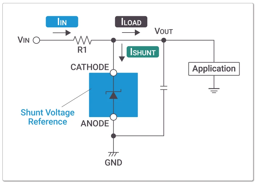
The figure on the right is a simplified circuit diagram showing a shunt voltage reference connected to peripheral components.
The shunt voltage reference has two pins: a CATHODE and an ANODE. A shunt resistor R1 is connected to the CATHODE pin, and the input voltage VIN is applied to the other end of R1. The output voltage VOUT is supplied from the CATHODE pin to the load or other applications.
Current Flow
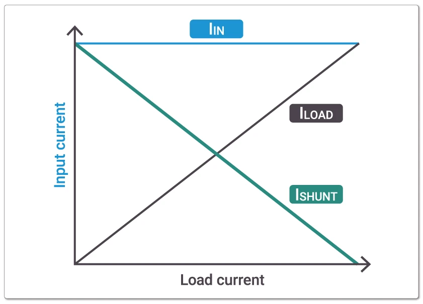
The input current IIN flows through the shunt resistor R1. IIN is the sum of the shunt current (ISHUNT) flowing into the voltage reference and the load current (ILOAD) flowing into the load.
If VIN is constant, even when ILOAD changes, the constant voltage operation of the voltage reference causes ISHUNT to vary inversely, keeping IIN constant. As a result of this operation, the output voltage equation becomes:
VOUT = VIN - IIN × R1
= VIN - (ILOAD + ISHUNT) × R1
By selecting the shunt resistor R1 so that VOUT equals the desired reference voltage, a stable reference voltage can be generated over a wide range of VIN.
Internal Configuration of Shunt Voltage References
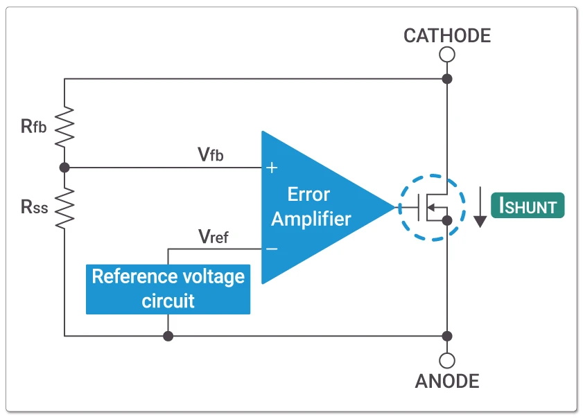
The figure on the right shows a simplified block diagram illustrating the internal configuration of a shunt voltage reference.
The internal structure of the shunt voltage reference primarily consists of a reference voltage source, an error amplifier, feedback resistors, and an output transistor.
The error amplifier compares the reference voltage (Vref) with the feedback voltage (Vfb), which is the VOUT (at the CATHODE pin) divided by the feedback resistors (Rfb and Rss). By controlling the output transistor, the error amplifier adjusts ISHUNT to maintain VOUT at a constant level.
Mechanism of Constant Voltage Operation
For example, if the load current (ILOAD) connected to VOUT (CATHODE) increases and VOUT decreases, the feedback voltage Vfb, divided by Rfb and Rss, also decreases. The error amplifier then controls the output transistor to reduce ISHUNT, causing VOUT to rise. Through this mechanism, a constant VOUT is continuously maintained.
Comparison with Zener Diode
The basic operation of a shunt voltage reference is similar to that of a Zener diode, in that it conducts current when the voltage across the CATHODE and ANODE exceeds a specific value, thereby keeping the output voltage constant. However, Zener diodes have a characteristic where the breakdown voltage varies depending on the current flowing through the diode itself. In contrast, a shunt voltage reference has an internal error amplifier that continuously monitors and controls the voltage. This enables the suppression of voltage fluctuations, allowing VOUT to be generated with higher accuracy than when using a Zener diode.
3. Try ABLIC's Shunt Voltage References
ABLIC's shunt voltage references for automotive use achieve the industry's highest* output voltage accuracy of ±0.1%, the industry's lowest* output voltage temperature coefficient of 20ppm/°C, and low output noise of 28μVRMS (when the output voltage is 2.048V).
Because they can supply a high-precision reference voltage even in harsh temperature environments, they contribute to improving the reading accuracy of electronic devices and sensor equipment. Furthermore, their low output noise and high output current enable simpler system design and overall cost reduction.
*Based on our research as of February 2026.
| S-19760 | Output voltage accuracy ±0.1% Output voltage temperature coefficient 20ppm/°C Maximum shunt current 15mA | ||
| S-19761 | Output voltage accuracy ±0.1% Output voltage temperature coefficient 20ppm/°C Maximum shunt current 30mA |