Table of Contents
1. The growing need for high-precision signal processing and high-speed ADC
 In recent years, advances in fields such as AI have required certain applications (medical imaging processing instruments, measuring instruments, industrial automation, etc.) to quickly recognize external analog signals and make decisions for the proper operation of the applications with a high degree of precision good. In the future, systems will be expected to require instantaneous image recognition, for example within factory automation machines which will require a higher level of data processing to keep up with the demands for elite recognition precision. Such systems contain physical information (analog signals) such as luminous intensity, temperature, and speed that are collected by sensors, converted to digital signals, and then passed to a signal processor that instantly executes a decision based on the signals received. Therefore, a high-speed AD converter (ADC) that converts analog signals into digital signals with higher precision and speed is essential for the latest cutting-edge systems.
ABLIC's ADC features high-precision and high-speed conversion, for example, when combined with ABLIC's ultrasound diagnostic equipment ICs, which have been used in medical institutions and clinics around the world for over 15 years, a medical system with high-speed, high-precision, and low power consumption is achieved.
2. Advantages of ABLIC's high-speed ADC
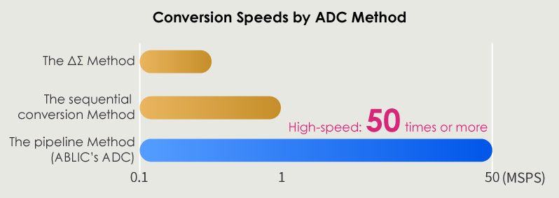
The pipeline method of ADC
The ADC is a major conversion method along with the ΣΔ and sequential conversion methods.
The pipeline method is characterized by high-speed and high-resolution, ideal for systems that require high-speed conversion, such as image processing.
Comparison of Conversion Speeds by ADC Method
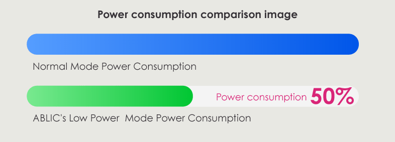
Low Power Mode
This mode is best suited for portable applications or battery-powered equipment that require low-power operation. When switching from Normal Mode to Low Power Mode, power consumption can be reduced by about 50%.
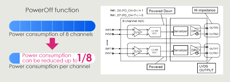
PowerOff function for each channel up to 8 channels
Each block of 8 channels can be powered down by one single channel. By commanding 1 to each bit of the associated register, the ADC, serializer, and LVDS driver of the corresponding channel will be powered down. Powering-down by a single channel enables precise power consumption control.
Automatic thermal protection using the indicator temperature setting can be configured
A temperature indicator detects abnormal overheating of the IC and the entire system. The detection temperature of the indicator can be selected in the register settings. The selectable detection temperatures are 110℃, 130℃, and 150℃.
A signal is instantly output when the IC detects an abnormal temperature for any reason. Optimizing the temperature setting reduces the risk of system failure or malfunction.
Double termination function and LVDS current value change function improves LVDS waveform quality
Double termination function
Impedance matching with the transmission wiring on both the LVDS transmitting and receiving sides, suppresses the effects of reflection in the transmission wiring.
It also suppresses output signal amplitude attenuation at high frequencies which can be caused by parasitic capacitance in the transmission wiring.
LVDS current value change function
Increasing the LVDS output current consequently increases the differential output amplitude voltage level. Suppressing the effects of disturbances in the transmission path.
At the same time, it suppresses output signal amplitude attenuation at high frequencies caused by parasitic capacitance in the transmission wiring.
It also eliminates misidentification of the LVDS interface and reduces noise due to overshoot.
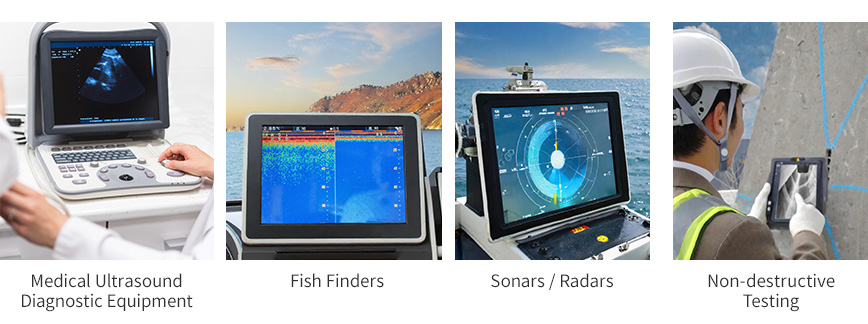
Application Examples
- Medical imaging processing equipment (ultrasound, CT, MRI)
- Measuring instruments
- Test and measurement equipment
- Non-destructive Testing
- Industrial automation
- Cellular phone base station
- Sonars / Fish Finders
- Optical communication devices
- Wireless communication devices

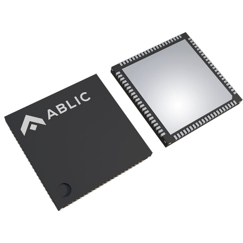
Octal ADC with LVDS Outputs S-US85A1
Features
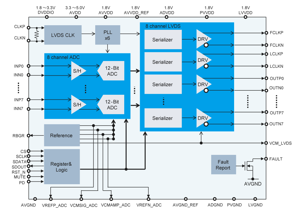
- 12-bit resolution 8-channel ADC in offset binary format
- 50Msps sampling rate
- 69.8dB SNR at 5.3MHz
- 78.8dBc SFDR at 5.3MHz
- Serial 300MHz LVDS output
- Offset binary digital code LVDS output
- Wide differential analog input 2.0Vp-p
- 1.8V to 3.3V CMOS control logic interface
- Selectable Normal and Low Power operation with register
- Normal mode 138mW/ch
- Low Power mode 78mW/ch
- 84-lead 10 × 10mm QFN package