Animation digest (Duration: 1:17)
 1. The development of IoT and wearable devices is proceeding at a rapid pace, however quick dying batteries are too common problems.
ABLIC's new S-85S1P Series DC-DC Switching Converter solves this problem.
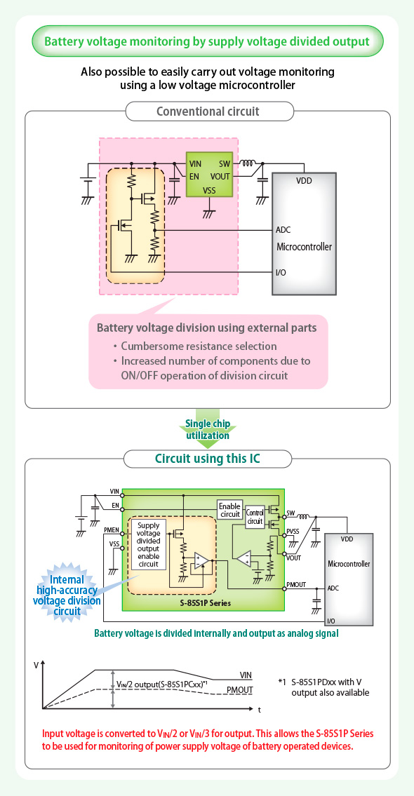
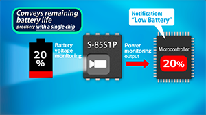 2. This IC features a supply voltage divided output, which monitors remaining battery life with a single chip. And it allows us to know when to replace the battery ahead of time.
 3. In addition, this IC maintains an ultra-compact profile,
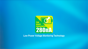 4. while allowing the supply voltage divider block to accommodate an ultra-low current consumption of 280 nA.
 5. “Easier to use, and more usable than ever.”
ABLIC contributes to the further development of comfortable IoT and wearable devices.
Innovation brought about by the collaborative creation with end users ── Ultrahigh-Efficiency Step-down Switching Regulator with a Supply Voltage Divided Output S-85S1P
ABLIC's S-85S1P is an ultrahigh-efficiency step-down switching regulator for which a supply voltage divided output is added to it’s recently introduced S-85S1A Series. Like the S-85S1A, the S-85S1P features ultra-low self-current consumption, fast transient response, space saving package and enables an accurate understanding of the remaining battery life with its supply voltage divided output.
Shaped by customer feedback
Along with the diffusion of mobile devices such as smartphones and tablets and now the expansion for the demand of IoT devices, the expectations for low power wireless modules such as Bluetooth Low Energy and LoRaWAN are increasing. In general, BLE modules and LoRaWAN modules are required to operate for a sufficiently long time, even with a small battery. For BLE modules, a supply voltage divided output is required to accurately ascertain the remaining battery life. When implementing a supply voltage divided output, because the self-current consumption has a negative impact on the running time of the battery for the entire module, the self-current consumption of the supply voltage divided output needs to be extremely low. Minimizing the self-current consumption of supply voltage divided output while accurately detecting the remaining battery life ── The company who requested a new solution from ABLIC to resolve these two challenges is Braveridge Co., Ltd. Braveridge is a startup that develops and produces IoT devices as well as develops and manufactures low power wireless modules such as BLE/LoRaWAN. To respond to the company’s request, ABLIC developed the S-85S1P, a step-down switching regulator that includes a supply voltage divided output. By adopting it, Braveridge succeeded in solving the two challenges it was facing.
Improvement of service design through supply voltage divided output
In general, to understand the remaining battery life, a separate monitoring circuit is typically required. However, this conventional method requires additional mounting space on the board because of the necessary external components. In addition, the accuracy is compromised. There is also the issue whereby the monitoring circuit on its own consumes power in order to ensure its accuracy. The supply voltage divided output feature within the S-85S1P divides the battery voltage input into fractions of half or one third. The S-85S1P then outputs and analog signal from the monitoring pin which can be input into the A/D converter terminal of the microcontroller.
 Architecture of S-85S1P
The self-current consumption of the supply voltage divided output circuit is reduced to 280 nA and is not more than 540nA total including the self-current consumption of the step-down switching regulator. Because the supply voltage divided output circuit can be disabled, it consumes only 260 nA for the main circuit when it is not monitoring. This allows the battery consumption of the voltage monitoring to be minimized. This supply voltage divided output can monitor the source voltage more accurately than existing circuits so it enables a precise understanding of the remaining battery life. It is possible to accurately predict the timing for replacing or charging the battery and to possible switch to an energy saving mode.
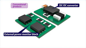
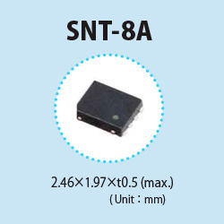 The S-85S1P does not require an external supply voltage divided output circuit and all elements are implemented in an ultra-small package, the SNT-8A. The SNT-8A dimensions are 2.46 x 1.97 x 0.5 mm, the industry’s smallest class. While it implements a supply voltage divided output circuit, it achieves space savings close to the S-85S1A in the SNT-6A package; (1.8 x 1.57 x 0.5 mm; 6 terminals). In addition, a variety of protection circuits are integrated as in the S-85S1A.
ABLIC has been developing various technologies to promote effective utilization of batteries, based on quickly identifying customers' potential needs. Giving shape to customers' thoughts ── ABLIC will continue to aim at providing products that satisfy the customers' requirements.
- S-85S1A/S-85S1P Series
Product brochure download 
COLUMN
- Vol.1 Do you know what it is? It is the secret to dramatically extending the battery life of wearable devices! (May 15, 2017)
- Vol.2 Self-current consumption of 260 nA achieved ── Ultra-High Efficiency Switching Regulator, Impact of S-85S1A (June 8, 2017)
- Vol.3 Innovation brought about by the collaborative creation with end users ── Ultrahigh-Efficiency Step-down Switching Regulator with a Supply Voltage Divided Output S-85S1P (June 27, 2017)
- Vol.4 The Age of the IoT ── Have you ever had problems detecting the movement of things? ~ Why are Hall Effect Switch ICs perfect for solving such problems? ~ (Dec. 7, 2017)
- Vol.5 The Transformation in IoT Devices brought about by Innovations in Hall Effect Switch ICs ── What is the impact of the S-5718, which can distinguish three states in one device? (Dec. 19, 2017)